(China (Mainland))

Product Summary
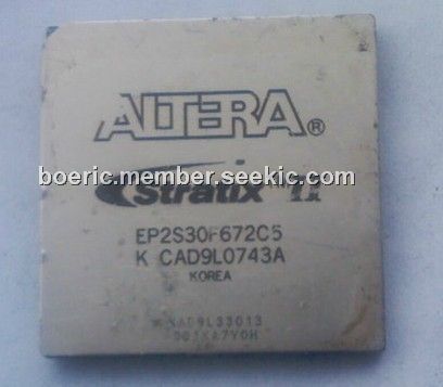
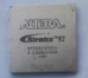
The EP2S30F672C5 is an FPGA based on a 1.2-V, 90-nm, all-layer copper SRAM process and features a new logic structure that maximizes performance, and enables device densities approaching 180,000 equivalent logic elements (LEs). The EP2S30F672C5 offers up to 9 Mbits of on-chip, TriMatrix memory for demanding, memory intensive applications and has up to 96 DSP blocks with up to 384 (18-bit × 18-bit) multipliers for efficient implementation of high performance filters and other DSP functions.
Parametrics
EP2S30F672C5 absolute maximum ratings: (1)VCCINT, Supply voltage With respect to ground: –0.5 to 1.8 V; (2)VCCIO, Supply voltage With respect to ground: –0.5 to 4.6 V; (3)VCCPD, Supply voltage With respect to ground: –0.5 to 4.6 V; (4)VCCA, Analog power supply for PLLs With respect to ground: –0.5 to 1.8 V; (5)VCCD, Digital power supply for PLLs With respect to ground: –0.5 to 1.8 V; (6)VI, DC input voltage: –0.5 to 4.6 V; (7)IOUT, DC output current, per pin: –25 to 40 mA; (8)TSTG, Storage temperature No bias: –65 to 150℃; (9)TJ, Junction temperature BGA packages under bias: –55 to 125℃.
Features
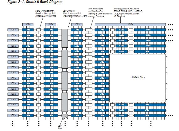
EP2S30F672C5 features: (1)15,600 to 179,400 equivalent LEs; (2)New and innovative adaptive logic module (ALM), the basic building block of the Stratix II architecture, maximizes performance and resource usage efficiency; (3)Up to 9,383,040 RAM bits (1,172,880 bytes) available without reducing logic resources; (4)TriMatrix memory consisting of three RAM block sizes to implement true dual-port memory and first-in first-out (FIFO) buffers; (5)High-speed DSP blocks provide dedicated implementation of multipliers (at up to 450 MHz), multiply-accumulate functions, and finite impulse response (FIR) filters; (6)Up to 16 global clocks with 24 clocking resources per device region; (7)Clock control blocks support dynamic clock network enable/disable, which allows clock networks to power down to reduce power consumption in user mode; (8)Up to 12 PLLs (four enhanced PLLs and eight fast PLLs) per device provide spread spectrum, programmable bandwidth, clock switch-over, real-time PLL reconfiguration, and advanced multiplication and phase shifting.
Diagrams
| Image | Part No | Mfg | Description |  |
Pricing (USD) |
Quantity | ||||||
|---|---|---|---|---|---|---|---|---|---|---|---|---|
 |
 EP2S30F672C5 |
|
IC STRATIX II FPGA 30K 672-FBGA |
Data Sheet |
|
|
||||||
|
EP2S30F672C5N |
|
IC STRATIX II FPGA 30K 672-FBGA |
Data Sheet |
|
|
||||||