(China (Mainland))

Product Summary
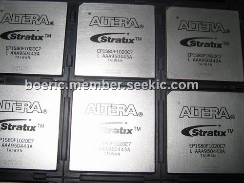
The EP1S80F1020C7 FPGA is based on a 1.5-V, 0.13-μm, all-layer copper SRAM process, with densities of up to 79,040 logic elements (LEs) and up to 7.5 Mbits of RAM. The EP1S80F1020C7 offers up to 22 digital signal processing (DSP) blocks with up to 176 (9-bit × 9-bit) embedded multipliers, optimized for DSP applications that enable efficient implementation of high-performance filters and multipliers. The EP1S80F1020C7 supports various I/O standards and also offer a complete clock management solution with its hierarchical clock structure with up to 420-MHz performance and up to 12 phase-locked loops (PLLs).
Parametrics
EP1S80F1020C7 absolute maximum ratings: (1)Supply voltage: –0.5 to 2.4 V With respect to ground, –0.5 to 4.6 V; (2)DC input voltage: –0.5 to 4.6 V; (3)DC output current, per pin: –25 to 40 mA; (4)Storage temperature No bias: –65 to 150 ℃; (5)Junction temperature: 135 ℃ at BGA packages under bias.
Features
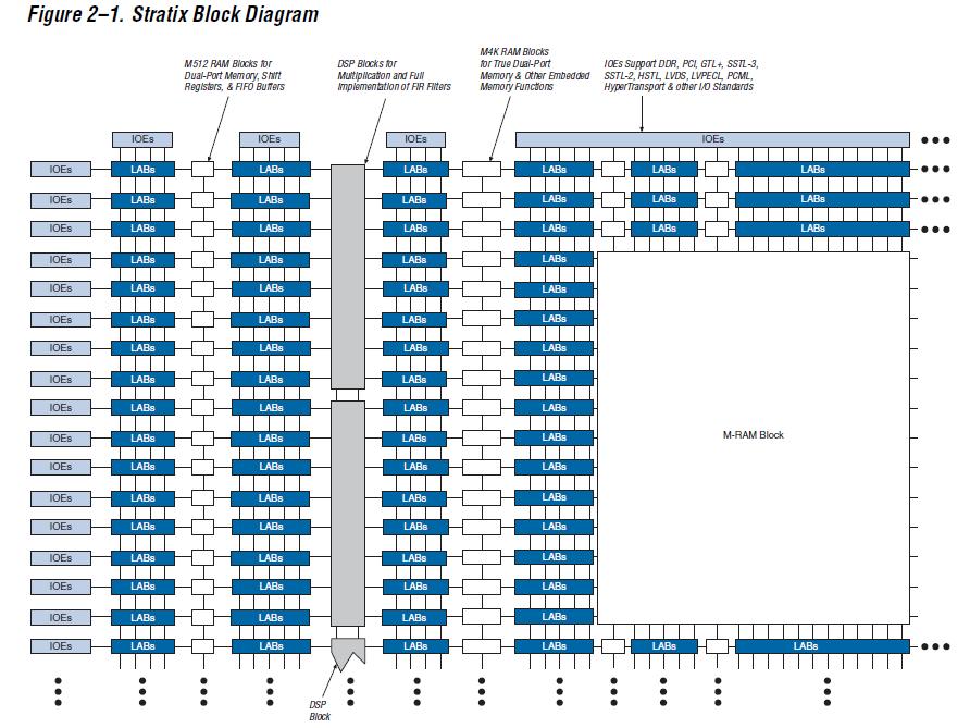
EP1S80F1020C7 features: (1)Up to 7,427,520 RAM bits (928,440 bytes) available without reducing logic resources; (2)TriMatrixTM memory consisting of three RAM block sizes to implement true dual-port memory and first-in first-out (FIFO) buffers; (3)High-speed DSP blocks provide dedicated implementation of multipliers (faster than 300 MHz), multiply-accumulate functions, and finite impulse response (FIR) filters; (4)Up to 16 global clocks with 22 clocking resources per device region; (5)Up to 12 PLLs (four enhanced PLLs and eight fast PLLs) per device provide spread spectrum, programmable bandwidth, clock switchover, real-time PLL reconfiguration, and advanced multiplication and phase shifting.
Diagrams
| Image | Part No | Mfg | Description |  |
Pricing (USD) |
Quantity | ||||||
|---|---|---|---|---|---|---|---|---|---|---|---|---|
 |
 EP1S80F1020C7 |
|
IC STRATIX FPGA 80K LE 1020-FBGA |
Data Sheet |
|
|
||||||
|
EP1S80F1020C7N |
|
IC STRATIX FPGA 80K LE 1020-FBGA |
Data Sheet |
|
|
||||||